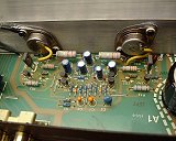
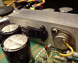
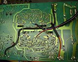
This page deals with technical aspects of the amplifier - construction, circuit details, faults and maintenance, etc. But before anything else, please read the following disclaimer:
The information provided on this page is 'as-is' for private study only. While every attempt is made to be accurate, the information is not guaranteed to be free from errors or applicable to all examples of the model.
Dismantling, servicing or modifying your amplifier carries many risks - the most serious hazard is the dangerous mains voltages present inside the unit which might cause injury or even death. Servicing or modifying the amplifier may result in damage to the amplifier and your loudspeakers.
The author disclaims all responsibility for any loss or damage and reading further implies agreement with this disclaimer. You have been warned!
Construction and disassembly
The top cover and front panel are extruded aluminium, and the bottom, sides and back panels are painted steel. The top and side panels overhang the rear by about an inch, which neatly hides the connectors from view - I think that is a really nice detail but I can recall at least one review criticising it, which seems rather petty to me.
Interior access is not easy; these units are not designed to be worked on! The side panels are easily removed, but you have to remove the top cover to access the main PCB. As the top cover is the heatsink, the amplifier can't be run for more than a few seconds without some other form of cooling, such as a fan.
The top panel is help on by 5 screws and the front panel (which is easily removed by undoing 3 screws underneath the unit). As you start to remove the top, you'll find that the heat-transfer compound will be gripping the aluminium U-section (which holds the output devices) quite effectively and some care is needed to separate them.
Important: Whenever this joint is disturbed, the two mating surfaces should be cleaned and a fresh layer of silicon heatsink compound should be correctly applied to one surface (see later). Do not dismantle your amplifier unless you have obtained some compound! Use a very thin even layer and ensure it covers the entire mating area.
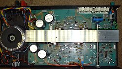 When I first took mine apart (2 days after
purchase ;-), I found that a heavy streak had been applied down the
length of the U-section which only covered 10-20% of the area - this
would result in poor heat transfer. From experience and feedback I've
received, I'm fairly convinced that this lack of quality-control at the
assembly-line has been the cause of many premature failures...
You'll want to clean up the heatsink compound straight away before it gets on your clothes and bench! Scrape it off with thick tissue paper or similar, then remove the last traces with your chemical of choice; I find that IPA works well. Having removed the top, you'll see the PCB.
Note that this picture shows my amplifier after I had serviced it (apart from changing the four main power supply capacitors). In the process, I tidied up the internal wiring slightly - don't be surprised if you find a birds nest inside yours!
Early MKI amplifiers have a two-part top panel, as you can see in the picture below (supplied by Frodo Muijzer). This is actually an A1-X, but as noted previously, this appears to be the European designation. Note that this model has ventilation holes in the side panels, suggesting that it is not one of the very earliest examples. If you have a two-part top cover, both halves need a layer of heat sink compound at their mating surfaces - something which appears to be mostly lacking in this example. The smoothing capacitors are axial and replacements might be hard to find today.

To remove the PCB, you need to remove two spacers towards the rear of the case and a number of M3 screws holding the PCB to the bottom panel. Next, free the rear panel from the bottom and remove the self-tapping screws from the PCB-mount phono sockets. Unbolt the 4mm phono earth connection. Finally, you'll need to free up the volume and input-select controls. Carefully remove the volume knob by rotating against the end-stop and pulling (it's a friction fit) and unbolt the potentiometer which is on flying leads. Then undo the front screw in the shaft-coupler and pull the input-select knob complete with extension shaft through the sub-front panel...
The PCB will now lift out, but pay special attention to the wires from the mains transformer, the speaker connections and the power LED.
As you can see, some reasonably good quality components are evident; for example most of the resistors are 1% metal film, and this was at a time when many competitors still used 5% carbon film. However, all the electrolytics are only 85°C rated, which somewhat surprised me!
Circuit Description
While servicing the amplifier some years ago, I took the opportunity to sketch out the schematic. You can download a scan of the hand-drawn circuit here. Use a graphics package to print it full-page - it should be reasonably clear, but I am working on producing proper electronic versions - honest!
As mentioned on the main index page, I have recently had conversations with Tim de Paravicini about the design, and the descriptions below have been updated in light of this.
Power supply
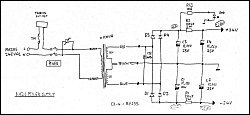 The
main power supply is relatively conventional - the mains supply is
presented to the toroidal transformer via a fuse, a thermal cut-out and
the power switch. A device that looks like a VDR is mounted on the power
switch...
The secondary windings produce ±24V nominally using discrete diodes and 2 reservoir capacitors. The second pair of capacitors is fed via 0.47Ω resistors which reduce ripple by a good amount - I measured 0.8V pk-pk across C3 and 0.25V pk-pk across C4. Possibly a cheaper version of the choke-regulated power supplies that MF use in more recent designs?
The smoothing capacitors are rated at 25V - rather close to the limit in my opinion!
Power amplifier
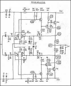 This is a curious design, in my
experience at least. It is a symmetrical design, using what appears to be
two identical amplifiers - indeed there are separate feedback paths for
each. You could replace one half of the amplifier with a suitable
current source and it would work happily...
At a glance, it might not look like a promising circuit, but the more you study it, the more elegant it seems. It's easy to be "put off" because it appears to be somewhat different to standard "textbook" layouts, but your patience will be rewarded!
Each half is very simple - essentially a long-tailed pair feeding the output device which is connected in a common-emitter configuration. The two intermediate transistors (TR7/8 and TR5/6) are simply emitter-followers, providing current gain...
The long tailed pairs are not fed from a current source, but the tail resistor is fed from a zener-regulated rail which prevents power supply noise reaching the LTPs. Each of the LTPs is unbalanced, meaning that the collector currents in each half of each pair are unequal. Maintaining equal collector currents with a current mirror or similar will provide the cancellation of second-harmonic distortion that is possible with a long-tail pair, but it's an option frequently eschewed by designers - mostly on cost grounds, but also perhaps because mild 2nd order distortion can sound "nice" subjectively.
As already mentioned, the next two transistors are emitter-followers and provide no voltage gain. Interestingly, each of these are only subjected to 25 volts worst-case, meaning that almost any transistor will do the job. And the various resistors (e.g., R16, R20) should protect the transistors in the event of problems with the output devices.
The output devices provide the second stage of voltage amplification. As they work in common emitter mode, the output is able to get relatively close to the supply rails(i.e. good "voltage efficiency"). Negative feedback is taken from the collector of each output transistor, and the loudspeaker output is taken from the junction of R30/31 (the two 0.22Ω resistors that are actually 0.47Ω in later and earlier models). The output impedance is set by the parallel impedance of these two resistors, giving stability and a defined damping factor.
What sets the quiescent current? You need to look to R30/31 for the answer. There is a small voltage across these resistors, and assuming that R30/R31 are accurate in value, you can determine that the standing current is 700mA approximately.
These small voltages are in fact DC offsets within each of the amplifier halves. Normally, one would "design out" DC offsets, but in this amplifier they are deliberately introduced by the 3M7 resistors (R6/11). Note that the exact values of these resistors might vary - and if your example uses 0.47Ω output resistors, expect to find something like 1M8.
The output devices are standard 2N3055/MJ2955 pairs - I'm told that no special selection or matching was required, and that Musical Fidelity relabeled them in an attempt to make the amplifier appear more "mysterious"; perhaps to ensure that their service department had to repair them (or sell transistors to the service trade). They were re-labeled "A1N" and "A1P" respectively, and a 4-digit date code was added - this confuses people because they assume it is part of the type number. Referring to my examples, my date codes are "9042" and "9034" - that means week number 42 and 34 of 1990. This form of date-coding is pretty-much industry-standard.
When replacing them, it's worth upgrading to the Motorola (On-Semi) MJ15003 and MJ15004 pair - these are more highly rated than the originals, and they should be much more reliable in the long term.
A quick note about the power supply arrangements. R13/14 drop the unregulated rails down to the Zener-regulated ±12V rails. These are separate for each channel, but the line preamp is based around a quad op-amp which is powered from these rails on the right power-amp. Hence, the left channel has higher values for R13/14 because of the reduced current demand. This also explains why the right channel disappears first at power-off...
A note about class A operation
The claim of class A operation has always been a controversial matter. It's worth pointing out that Musical Fidelity say that the amplifier is "strongly biased into class A", so apart from the lettering on the front panel (!), they have never claimed that the amplifier is a pure class A design as far as I can establish.
Many commentators, myself included, have analysed this amplifier on the assumption that it behaves exactly like a standard class AB design. In which case, one simply takes the standing current and doubles it to arrive at the peak current available in class A mode. This is then divided by root-2 to find the RMS current, then squared and multiplied by the load impedance to give the maximum continuous sine-wave power. The standing current in my example is 700mA which gives almost exactly 8 watts of class A operation into 8Ω - above this power, or at lower load impedances, the amplifier should revert to class AB. And allow me to quote from a Hi-Fi News review by Dave Berriman, published in the January 1994 issue. This review was admittedly of a mark 3 model (see below), but it's useful information anyway:
Out of curiosity, we checked the quiescent current through the output transistors. At 0.71A, this is enough for up to about 8W of pure Class A, which implies that over 8W the A1 runs into Class A/B.
Dave Berriman
Having said that, Tim de Paravicini argues that this approach doesn't apply to the A1. Quoting directly:
As to Class A, people cannot get into their minds the analogy with tube amps and realise that the two halves of the circuit are additive so that total available current is 1600mA [he assumes a standing current of 800mA] and the peak is about 2.3 amps. Power consumption of a push-pull class A amp is 50 percent efficient so 20 watts per channel times 2 is 80 watts from the mains. As a final proof, if the amp is driven into an 8 Ohm load with a sine wave at full output the heat sink temperature fell by more than 10 degrees. Because 40 of these watts is now in the load.
Tim de Paravicini
At this stage, I have to confess that I'm one of these people! Since reading this, I haven't been able to access my amplifier for testing because it is in storage - therefore all of my "experiments" have been on paper - and I have yet to discover how it might behave differently from a normal class AB design. In the future, I fully intend to (a) learn how to use Spice properly and (b) test my A1 once it's no longer in storage - in the meantime, I'm happy to report that Jez Arkless (mentioned on the index page) independently concurs with Tim - he's observed that the power consumption of the amplifier remains at 80 watts at both idle and when driven at nearly full power. That said, he reports that this is only true for the A1; all other "A series" amplifiers show increased power consumption at higher output powers as they enter class AB operation.
Line preamp
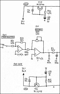 A TL084 op-amp forms the preamp. Two
sections are used per channel, both working in inverted mode. The first
section sets the basic input impedance to 47K, and has a gain of -3dB.
The second section incorporates the volume control in the feedback path,
and has a maximum gain of 20.5dB.
The basic problem with this preamp is that the volume controls, and input switches for that matter, get very noisy very quickly in the A1. In my case, I first noticed hints of this at just a month, and by a year, it was distinctly noisy in normal operation. This is a design problem - if you are tempted to replace the potentiometer and switches in yours, don't bother!
The problem is DC currents on the potentiometer and the input switches. Obviously, these currents are tiny - after all, the TL084 is a JFET input op-amp so the currents are as a result of input offset voltages - but they are there, nonetheless.
Tim de Paravicini had this to say:
The "Active Volume control" was dictated to me as part of the brief. Cheap pots and other parts let it down.
Tim de Paravicini
My first reaction was that I didn't consider an Alps "Blue" potentiometer to be cheap at around £10 from Farnell! It seems that early models used a cheap pot, and perhaps that's what he had in mind, but it seems that MF switched to this part because the standard-grade carbon potentiometers became noisy too soon. Evidence for this theory can be seen on the main PCB, which is laid out to accept a standard (cheap) potentiometer - the expensive Alps pot is fitted using flying leads. Furthermore, the B200 - a more expensive class AB MOSFET amplifier built in an identical case - uses the cheap £1 pot. Needless to say, the B200 uses a conventional arrangement with no DC on the track, and the potentiometers are much, much more reliable...
Another problem with this arrangement is the Johnson noise caused by the high resistances seen by the two op-amp sections. Note also there is no ultrasonic filter on the input, which could cause compatibility problems with some digital sources...
The supply for this stage is taken from the ±12V rails of the right power amp, as discussed above. They are fed via the active filters T17/18, which take a few seconds to come up. Ever switched on the amp with a source playing, and wondered why you get a burst of music (always at much the same level), then silence, then the music at the expected level? When first switched on, the power-amps work almost instantly, but the op-amp is not yet powered. So, the audio signal travels straight via R33, R32, R34 and the volume pot. As the rails start to rise, the op-amp wakes up and the signal is muted until the rails become further established...
Phono preamp
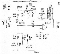 Remember when integrated amplifiers had
phono stages? This one even has an MC setting. It's slightly unusual in
that it has a transistor pre-amp prior to the op-amp, and this provides
the extra gain required for the MC option. It's quite neat - selecting MC
(via the rear-panel switch) increases the gain by reducing the emitter
resistance (at AC), simultaneously reducing the input impedance to
provide the correct loading for the cartridge.
The first stage is TR16, which is a transconductance amplifier (voltage in, current out). The op-amp - another TL084 - acts as a transimpedance stage, converting the input current into a voltage output while performing the RIAA equalisation. TR15 is an active load; the bottom end of R56 is bootstrapped by any signal voltage present being transferred to the base of TR15 via C30. This has the effect of raising the value of R56 "seen" by the signal, maximising the gain. The DC conditions are established by the 3k3 (which is R57 - apologies for missing the designation in the sketch) plus R58 and R40. As the base of TR16 is held at very close to ground, there is 11.7V across this combined 3k576, giving 3.3mA. There is 6V across R56, and the emitter voltage of TR15 should be around -10.4V, so the collector voltage of TR16 should be around -4.4 volts.
Phono preamp power suppy
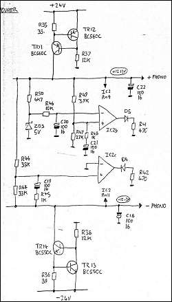 The power supply is rather more involved...
Initially I wasn't sure why this complicated arrangement was chosen in preference to cheap 7812 regulators, but the more you think about the phono stage, the more apparent it becomes that the transistorised front end has a very poor power-supply-rejection-ratio. In other words, any noise on the supply appears on the output. For clues, just look to C27/R40. This suspicion has since been confirmed by Tim de Paravincini.
TR11/12 and TR13/14 are current sources, feeding the quad op-amp. This device is able to influence the supply rails by sinking/sourcing current via its output stages - diodes D5/D6 ensure that IC1b only affects the positive rail and IC1c can only control the negative rail.
The surrounding circuitry is rather like you'd find in 'discrete' supplies - for example linear bench power supplies. ZD3 forms a reference voltage which is filtered by R46 and C20 - the -3dB point is around 0.16Hz. Because of the bass boost built into the RIAA curve, low-frequency noise must be minimised at every opportunity.
This reference is multiplied by ratio of R49/R47 plus 1 to determine the positive rail. As R44 and R46 are the same value and the negative reference is ground, the negative rail will accurately mirror the positive rail.
Mark III Models
Thanks to Nicolas Hodges, I've recently had the opportunity to examine a Mk 3 example. It is broadly similar to the earlier models, with the following changes:
- Power supply: extra smoothing capacitors and improved separation between the two channels.
- Power amplifier: minor component value changes.
- Line preamp: a rudimentary power-on mute circuit added.
- Phono preamp: Unchanged.
- Phone preamp power supply: the discrete arrangement has been dropped in favour of 78L12/19L12 regulator ICs
- PCB: lots of minor changes - the power supply and grounding arrangements have been improved, and the amount of internal wiring is reduced slightly. Interestingly, the PCB is marked "DAVID II" (see later)
One day, I'll post full details and pictures of this.
Final Edition
The Final Edition is substantially different... it's actually a B200, which is a class AB MOS-FET based amplifier. Ignoring the B1, Musical Fidelity had two basic amplifier topologies at the time - the bipolar design described above, and the opamp-plus-MOSFET topology that was used in most of their expensive models.
Please note - this schematic is based on a B200 that I serviced some years ago, and there are some slight differences to the version used in the A1. Also, there are some errors in the schematic, especially concerning TR5 and TR6, so use with caution! I have since repaired another B200, and confirmed all this - one day I'll upload corrected diagrams and more details of the B200.
The input signal from the tape monitor switch is applied directly to the volume control in a conventional manner. This is the first plus-point here, because it fixes the problem with the original preamp - noisy controls are very rare with this circuit.
From there, the input is applied to an LM318 op-amp, an elderly, but respectable high-speed device. This stage amplifies and inverts the signal, but the voltage swing at the output of the op-amp is limited by the power supply rails. To develop enough voltage swing to drive the loudspeakers, the output stage requires some gain. This is provided by TR6 and TR6, and the MOS-FETs themselves.
Despite what my diagram incorrectly shows, TR5 and TR6 are actually arranged as common-base amplifiers, which provides some of the gain and the necessary level-shifting. The MOS-FETs are arranged as inverting common-source amplifiers, which provides more voltage gain.
The supply to the op-amp is provide by 13mA current sources TR1, 2 and TR3, 4. ZD1 and ZD2 regulate the voltage rails to 12V. Earlier amplifiers using this layout used simple resistors instead of current sources, but these are a welcome addition. I recently received an email from someone who was successfully running his European B200 in the US where the mains supply voltage is only 120V. VR1 is used to adjust the quiescent current.
You'll note that there are a good number of small capacitors dotted around for HF compensation. Stabilising amplifiers with such unusual gain structures is not trivial, so I would advise caution when considering any modifications.
From memory, I the B200 I serviced had an exciting, powerful sound quality. It certainly plays a lot louder than the A1, as it was rated at 60 watts per channel (and gives a lot more than that in practice). The 40WPC A1 FE has lower power supply rails and a higher quiescent current. One criticism - the signal to noise ratio of the B200 wasn't that good, so if you plan to use it at low levels with efficient speakers, you might find noise and hiss to be a problem. Later models used a modification which is derived from a National Semiconductor application note, whereby an external long-tail pair is used and connected to the compensation pins of the LM318, and this somewhat reduces the noise of the amplifier.
What goes wrong?
These amplifiers have a reputation for unreliability, but given the operational temperatures, it's not surprising.
Noisy pots and switches
The bane of my life! It's so embarrassing to have a half-decent hi-fi with an unusable volume control! The failure mode is deposits on the track, particularly at the lower end of the scale. Unfortunately, the design of the preamp compounds the problem: as the wiper hits dirt and goes high-resistance, the volume is effectively max'd for a brief time. If the configuration was conventional, the sound would do the opposite, making the effect much less objectionable.
Also, the switches are affected for the same reason - the input op-amp stage puts dc currents through the switches. Replacing the pot and switches is a short-term solution. If you retain the original preamp, the new components will go the same way. See the modifications page...
Faulty electrolytic capacitors
This is the second big problem with these amplifiers. Heat is a major enemy of electrolytic capacitors, so it will be no surprise to hear that they are a particular problem with this amplifier! The original components were of fairly average quality to begin with, which clearly doesn't help.
Look in an electronics component catalogue, and you'll see that electrolytic capacitors have a finite life expectancy, typically around 2000 hours for a standard quality device. This is quoted at an operating temperature of 85°C, and as a rule of thumb, reducing the operating temperature by 10 degrees will double the life expectancy. As the surface of the heat sink is around 60-65°C, the internal temperature will be even higher. Remember, 2000 hours might sound like a lot, but that's only 2 years if you use the amplifier for 3 hours a day!
The symptoms of faulty capacitors are hard to predict. Basically, it only takes one degraded capacitor to affect the performance of the circuit, and as it's hard to detect a gradual change in sound quality, you can be forgiven for not noticing faults developing. When they get particularly bad, it's possible that other components can fail as a result of the changes operating conditions within the amplifier. The message is simple - if you have a fault with the amplifier, don't start trying to apply logic until you've replaced all the capacitors. In 95% of the cases I've come across, this will clear the fault.
Better quality capacitors will be rated at 105°C, and will have a longer life span as well. Follow the logic of doubling the life span with every 10°C fall in temperature, and you'll soon see why fitting anything less is a false economy.
Remember to look for long-life, low-ESR, 105°C rated capacitors - Rubycon YXF, Elna RJH or Panasonic FC are all good starting points. I'd steer clear of "exotic" or "boutique" components like Black Gates as they're only rated at 85°C - it seems perverse to spend a fortune on capacitors that will be no more reliable than the originals.
It took me a little while to locate the main reservoir capacitors because of the limited space - they can only be 25mm high. From the Panasonic HA series, the 10,000uF, 25V 105°C fits the bill and is readily available from the usual suppliers.
You can replace C6 and C7 with 1µ non-electrolytics, but they have to be physically small.
Needless to say, you need to be very careful about the polarity of all the electrolytic capacitors. There are markings on the PCB, and you can check against the schematic...
Failed output stages
Not surprisingly, the output devices can expire as a result of the long-term heating, not helped by the poorly applied thermal compound. Luckily, this amplifier is relatively "fail safe", and not prone to the catastrophic failures that affect many audio power amplifiers, where failure of an output device normally leads to cascaded faults further back in the circuitry - which is one reason why service centres are often reluctant to take on faulty amplifiers. But having said that, you should carefully check every active and passive component in the power amplifier stage before re-applying power. And make sure your speakers are not connected!
As there is no dc protection circuitry, a faulty output stage will probably damage loudspeakers if there is significant dc offset present... Maplin sell (sold?) a Vellemen kit (K4700) that protects the speakers from the amplifier under these circumstances, and is definitely worth adding if possible...
About that heat sink compound...
 If you're considering servicing
one of these, it's important to know how to re-apply this thermal
compound. Of course, you have to do this whenever you remove the top
cover, so if you fancy having a nose "under-the-hood" of your
amplifier, but aren't brave enough to do anything more drastic, this
might improve long-term reliability...
This picture shows you how best to reapply the compound before reassembly. Obviously, all the old compound has already been removed from the U-section and the top panel. Using a straight edge, the compound has been spread evenly in a thin layer, avoiding the screw holes and the outer few mm. It's important to realise that the grease is intended to fill the microscopic gaps in the mating surfaces - you are not trying to "paint" the aluminium white! When reassembled, a small amount of compound escaping from between the joint indicates a good distribution...
Another point to check is the torque of the screws holding the output devices. Don't overtighten them, but make sure they aren't loose.
After re-assembly, you might want to check the torque of the three U-section bolts once the amplifier has warmed up. Don't apply masses of pressure as you might strip the threads in the aluminium U-section, but do make sure they are 'nipped-up' securely...
Remember that if your top cover is in two sections, you must apply compound where the two halves meet!

