 The subject of this page is the inability to
trigger on any signals, caused by the failure of IC1 in the timebase
circuit. I've put the remaining faults on a separate
page...
The subject of this page is the inability to
trigger on any signals, caused by the failure of IC1 in the timebase
circuit. I've put the remaining faults on a separate
page...
IC1 Failure
This IC was custom-made by Tektronix, who owned Telequipment at this point, and it was only used in this model (and the D63, the non-storage version of the DM63). It had apparently failed a couple of times before, so you could be forgiven for thinking that it's not very reliable, but having said that, I haven't heard of another instance of IC1 failing since posting this information back in 2002. During that time, I have had a lot of correspondence regarding this model, but IC1 has remained resolutely blameless. So I now suspect that there was another fault with my scope. Looking at the diagram it's easy to see how a problem in the preceeding stage (TR2, etc) could damage the IC.
With that in mind, the information about my repair is presented here for interest; or inspiration, if you prefer. Proof that anything can be repaired if you really want to! I have no plans to produce a presentable copy of the schematic at this time - it would simply take up effort that would be better spent elsewhere.
Anyway, my only option was to design a replacement circuit for IC1. It has to do a reasonable amount - in addition to accepting the analogue trigger signal and controlling the sweep generator (IC2), all timebase functions, such as auto-bright-basline, holdoff, single-sweep and X-Y lockout are controlled by IC1. I began by running a ribbon cable from the IC socket to a prototype board. This evolved into a Veroboard prototype (which worked well for about 7 years). Then, as part of a total overhaul, I decided to fix the final bugs and produce a PCB version.
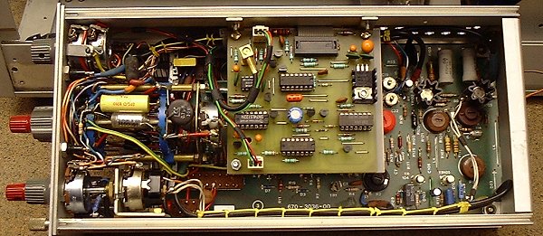
Veroboard prototype
This bodge served me well enough for a good few years, but was not perfect. The performance of the comparator could have been better (Veroboard is not exactly the ideal medium for high frequency circuitry, of course), and at fast sweep-rates, you'd get double-imaging and instability. I found later that these problems were caused by insufficient hold-off time; obviously it's hard to measure this without another 'scope!
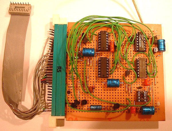
Once these and other minor details had been sorted, I was able to think about producing a PCB version.
Trigger signal conditioning
Before comitting to a PCB, it made sense to think carefully about perfectly integrating the new circuity with the existing instrument, which in turn led me to spend a long time studying the analogue trigger circuitry surrounding IC1. The various signals are switched by diodes and inverted by a single-transistor preamp stage (TR2), before level-shifting diodes apply the signal to the IC...
I borrowed an old Telequipment D83 from work. This is a 50MHz oscilloscope in a similar chassis to the DM63, and it enabled me to make the detailed measurements that I needed for this project. Pretty quickly, I decided that TR2 (handling the trigger signal ahead of IC1) was limiting the bandwidth excessively and had to go. OK, the original IC is only specified to 15MHz, so I guess that's why its preamp wasn't exactly engineered for speed, but as the LS/HC TTL logic I was using is capable of working to at least 40MHz, it seemed silly to throw away potential performance. Yes, the Y-amps in the DM63 are only specified to 18MHz, but that just means that amplitude readings become inaccurate above this frequency; it's still useful to be able to lock to higher frequencies.
The trigger amps in the plug-ins expect a 75 ohm load. I removed TR2 from the timebase board, and connected a 75 ohm resistor in its place. I then developed a better preamplifier, which used 5 transistors, had a gain of around 10, and was pretty flat up to at least 30MHz (the limit of my Wavetek function generator).
Next to think about was the comparator, and I decided to see if there was a better option than the IC used on the Veroboard prototype. A little bit of research led me to a device made by Maxim. The MAX909 has built-in trigger-points set at ±2mV - this means no external resistors to worry about. This got me thinking - the low threshold points will result in good sensitivity, better than I would have risked if I was using external components to set the hysteresis in the conventional manner. Just how necessary was my pre-amp?
A breadboard test revealed this device gave excellent results - trigger sensitivity was around 0.2-0.3 divisions at L.F. (better than any scope that I was able to test at work), and it performed well up to at least 30MHz. It also didn't seem to suffer from spurious triggering (the danger with an over-sensitive comparator). So this IC enabled me to drop a whole load of analogue circuitry, providing an easy solution to a potentially tricky problem...
Please note that Maxim have discontinued the MAX909, replacing it with the MAX9109. Inevitably, it's only available in surface-mount packages!
Mechanical modifications
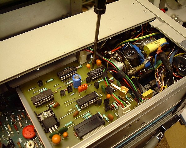
I removed the timebase module and stripped it down for easy access. As a result of the removal of the preamplifier, a total of 26 components were removed from the PCB:
Some minor modifications to the metalwork were required. Two holes in the top panel hold the PCB via small right-angle brackets. While I was at it, I drilled some holes above the X-output stage to help improve ventilation. The copper-clad board offers screening from the fast-edged TTL signals that float around the board. A sheet of insulating plastic is essential, of course...
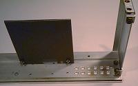
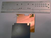
The cut-out in the copper-clad board was already there, but by chance it fits perfectly with the ribbon cable that connects to IC1's socket. The analogue trigger signal enters the board via a short length of cable and an SMB plug. This is terminated with a surface-mount 75Ω resistor directly under the socket on the PCB. This works well, despite the SMB connector (and cable) being 50 ohms; I guess 30MHz is still DC as far as these are concerned!
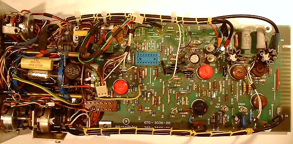
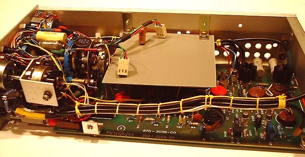
This picture show how the new PCB fits into the timebase chassis. The two Molex connectors are for the front-panel LED and ±24V power supply. The existing 5 volt power supply (a BC109 and zener diode) has been removed from the main PCB, replaced by a 7805 on the new board. Also, the 'single-sweep ready' LED and connections have been removed in favour of a dual-colour device: in addition to the normal red "Ready" LED, there is a green "Triggered" indication...
This shows the (almost) completed board. The hole between the two tantalum capacitors (bottom left) is to enable adjustment of R2 on the main PCB without having to remove the board.
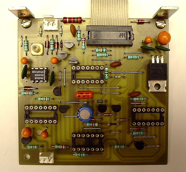
The layout might not look all that compact, but I really did get the board as small as possible without going to much tighter design-rules. The main priority was to ensure the board was easy to etch and assemble.
After taking this picture, I added a small heatsink to the 7805. It only dissipates a watt or so, but my cheap indoor/outdoor thermometers claim the ambient temperature near this board is in the 60-65°C region with the covers on. The only other components that get warm are the three power supply dropper resistors near to the top-left Molex connector. TTL doesn't generate significant heat in applications like this...
This shows the final timebase assembly, just before installation back into the 'scope. I think it's worked out really well - there's just enough slack on the cables to operate the unit with the additional PCB hanging to one side for access, and it doesn't look too much like the total bodge that it is!
Finally, this picture shows how the hole (mentioned above) enables adjustment of R2 without disassembly. That worked out perfectly, but I have to admit that luck was on my side as it was quite hard to make accurate measurements...